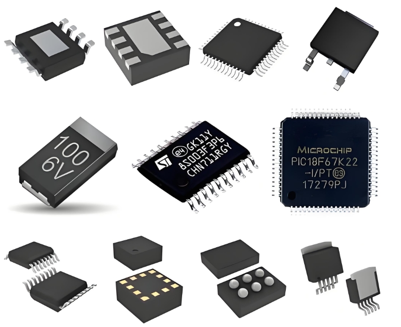
**The HMC1110: A Comprehensive Guide to Its Operation and Applications in Modern RF Systems**
The relentless drive for higher performance and integration in radio frequency (RF) systems has made advanced semiconductor components indispensable. Among these, the **HMC1110** stands out as a critical enabler for modern communication and radar applications. This article provides a comprehensive overview of the HMC1110, detailing its operational principles and showcasing its pivotal role in contemporary RF design.
**Understanding the HMC1110: A High-Performance RF Building Block**
The HMC1110 is a **silicon germanium (SiGe) monolithic microwave integrated circuit (MMIC)** designed and manufactured by Analog Devices. At its core, it is a **wideband, non-reflective SPST switch**. Unlike traditional reflective switches, which direct unused RF power back to the source, non-reflective switches terminate this power into a matched load. This key characteristic is crucial for protecting sensitive components like **low-noise amplifiers (LNAs)** and oscillators in a system chain from damaging reflected power, thereby enhancing overall system reliability and linearity.
The device operates over an exceptionally broad frequency range, from **DC to 20 GHz**, making it incredibly versatile for numerous bands and standards. It offers excellent RF performance, including low insertion loss (typically <1 dB), high isolation (typically >40 dB at 10 GHz), and the ability to handle high input power levels (up to +29 dBm CW). Its fast switching speed of approximately 6 ns is vital for applications like Time Division Duplex (TDD) systems and pulsed radar.
**Operational Principles: How the HMC1110 Functions**
The operation of the HMC1110 is governed by a single control voltage pin (V_CTRL). Applying a positive TTL-compatible voltage (typically +3V to +5V) puts the switch in the "ON" state, creating a low-loss path between the RF input (RF1) and output (RF2) ports. In this state, the internal FETs are configured to allow signal passage.
Applying 0V or a negative voltage (down to -3V) to V_CTRL places the switch in the "OFF" state. Here, the signal path is broken, and the RF input is terminated to ground through an integrated 50-ohm resistor. This termination is the defining feature of its non-reflective architecture. The negative voltage swing enhances the power handling capability of the switch by ensuring the internal FETs remain fully pinched off when subjected to high-power RF signals.
**Key Applications in Modern RF Systems**
The combination of wide bandwidth, high power handling, and non-reflective design makes the HMC1110 suitable for a vast array of demanding applications:
1. **TDD Wireless Infrastructure:** In 5G NR base stations and other TDD systems, a single antenna is shared for transmission and reception. The HMC1110 is ideal for the **Transmit/Receive (T/R) switch**, swiftly routing high-power signals from the power amplifier to the antenna and then protecting it by connecting the antenna to the sensitive receiver LNA during receive cycles.
2. **Electronic Warfare (EW) and Radar Systems:** These systems require switches for **beamforming networks**, **attenuator arrays**, and channel selection. The HMC1110's fast switching speed is critical for **frequency hopping and pulse routing**, while its high isolation prevents signal leakage between channels.
3. **Test and Measurement Equipment:** High-performance signal analyzers, vector network analyzers, and automated test equipment (ATE) use the HMC1110 for **signal routing and multiplexing**. Its wide bandwidth allows a single switch to cover multiple frequency bands, simplifying instrument design.

4. **Satellite Communications (SATCOM):** In phased array antennas for SATCOM terminals, thousands of elements require precise control. The HMC1110's small size, high performance, and reliability make it a strong candidate for **phase shifter and attenuator control circuits** within these arrays.
**Design Considerations**
Integrating the HMC1110 requires careful attention to a few key areas:
* **Biasing:** Providing a clean, stable negative voltage is essential for optimal performance, especially for high-power operation.
* **PCB Layout:** Implementing a **high-quality RF board layout** with continuous ground planes, appropriate via fencing, and matched 50-ohm microstrip lines is paramount to achieving the specified performance.
* **ESD Protection:** As a sensitive MMIC, proper handling and board-level ESD protection measures should be employed.
**ICGOODFIND**
The HMC1110 represents a cornerstone component in high-frequency design. Its **non-reflective architecture, exceptional bandwidth from DC to 20 GHz, and robust power handling** capabilities solve critical challenges in protecting sensitive components and managing high-power RF paths. From enabling the dense infrastructure of 5G to ensuring the reliability of advanced radar and electronic warfare systems, the HMC1110 proves to be an versatile and powerful solution for RF engineers pushing the boundaries of performance.
**Keywords:**
1. **Non-Reflective SPST Switch**
2. **Monolithic Microwave Integrated Circuit (MMIC)**
3. **Wideband DC to 20 GHz**
4. **Transmit/Receive (T/R) Switching**
5. **High Power Handling**
